BEU B.Tech CSE Analog Circuits Module 1 Notes
Complete BEU B.Tech CSE Analog Circuits Module 1 notes with clear explanations, diagrams, formulas, and exam-focused content. Useful for AKU semester students preparing for Analog Circuits.

If you are a BEU/AKU B.Tech CSE student, finding clear and well-organized academic notes for your semester can be difficult, especially for subjects like Analog Circuits in Module 1. This page brings you complete B.Tech CSE notes, semester-wise notes, and AI & ML friendly explanations designed to help you understand the core topics faster. These Analog Circuits Module 1 notes include definitions, diagrams, formulas, and previous-year important concepts so you can prepare for exams with confidence. Whether you are searching for BEU B.Tech notes, CSE study material, AKU semester notes, or AI/ML-oriented analog electronics notes, you will find everything in an easy and student-friendly format here.
What is a Semiconductor
A semiconductor is a special type of material whose ability to conduct electricity is between that of a conductor (like copper) and an insulator (like rubber).
It does not allow current to flow freely like a metal, but it also does not block current completely.
Its conductivity changes based on temperature, impurities, and external conditions, which makes it very useful in electronic devices.
Semiconductors are the building blocks of almost every electronic component such as diodes, transistors, ICs, LEDs, solar cells, and sensors.
Important Points
Conductivity lies between conductor and insulator.
Conducts more when temperature increases (opposite of metals).
Its properties can be changed by adding impurities (doping).
Most commonly used semiconductor materials are Silicon (Si) and Germanium (Ge).
Almost all modern electronic devices are made using semiconductors.
Can behave like a conductor or insulator depending on conditions.
Why Semiconductors Are Important
Semiconductors allow us to control the flow of current.
This ability to control current makes it possible to design:
Switches
Amplifiers
Digital logic circuits
Microprocessors
Memory chips
Power control circuits
They are at the heart of all modern electronics.
Types of Semiconductor Materials
Intrinsic semiconductor – pure semiconductor without impurities.
Extrinsic semiconductor – semiconductor with added impurities to improve conductivity.
Intrinsic Semiconductor
An intrinsic semiconductor is a pure semiconductor material that does not contain any added impurities. It is made only of a single element such as pure Silicon (Si) or pure Germanium (Ge).
Because it is pure, its electrical conductivity is naturally very low at room temperature.
In an intrinsic semiconductor, the number of electrons (negative charges) and holes (positive charges) is always equal.
This balance happens because both electrons and holes are created only due to thermal energy (heat), not because of impurities.
Important Points
Made of pure semiconductor material with no impurities.
Examples: pure Silicon and pure Germanium.
Electrons = Holes (equal number of carriers).
Conductivity is low at room temperature.
When temperature rises, more electrons gain energy and break free → conductivity increases.
Current is carried by:
Electrons (in conduction band)
Holes (in valence band)
No doping is done in intrinsic semiconductors.
How Current Flows in Intrinsic Semiconductor
When thermal energy breaks a covalent bond, one electron becomes free.
The empty bond left behind is called a hole.
Free electrons move → electric current.
Holes appear to move in the opposite direction → hole current.
Total current = electron current + hole current.
Why Intrinsic Semiconductors Are Not Used Directly
They conduct very little current at room temperature, so they are not suitable for making practical electronic devices.
To improve conductivity, impurities are added → this creates extrinsic semiconductors, which are used in diodes and transistors.
Simple Real-Life Comparison
Think of an intrinsic semiconductor like plain sand:
It is natural and pure.
But it cannot build a strong structure on its own.
You must mix cement/gravel (impurities) to create strong concrete.
Similarly, intrinsic semiconductors need doping to become useful.
Extrinsic Semiconductor
An extrinsic semiconductor is a semiconductor whose conductivity is improved by adding a very small amount of impurity.
This process of adding impurity is called doping.
By doping, we can increase the number of free electrons or holes, which makes the material much more conductive and useful for making devices like diodes and transistors.
Because extrinsic semiconductors have more charge carriers, they are the actual materials used in electronic components.
Important Points
Formed by adding impurities to a pure (intrinsic) semiconductor.
Doping increases the number of free charge carriers.
Conductivity is much higher than intrinsic semiconductor.
Two types are formed: P-type and N-type.
Only a tiny amount of impurity (1 atom per 10⁸ atoms) is added.
Doping does not change the structure, only increases carriers.
Used to make diodes, transistors, ICs, solar cells, LEDs.
Why Do We Add Impurities?
Intrinsic semiconductors have very few free electrons or holes at room temperature.
So they cannot conduct enough current to be useful.
By adding impurities:
We can increase electrons → form N-type semiconductor
We can increase holes → form P-type semiconductor
This makes the material highly suitable for electronics.
Types of Impurities Added
Pentavalent atoms (5 valence electrons)
Example: Phosphorus, Arsenic
→ create N-type semiconductor (more electrons)Trivalent atoms (3 valence electrons)
Example: Boron, Gallium
→ create P-type semiconductor (more holes)
How Current Flows in Extrinsic Semiconductor
In N-type, electrons are the majority carriers → they carry current.
In P-type, holes are the majority carriers → they carry current.
Minority carriers also exist but in very small numbers.
Simple Real-Life Comparison
Adding impurity to a semiconductor is like adding salt to water:
Pure water conducts almost no electricity.
Add a small amount of salt → conductivity increases a lot.
Similarly, a small amount of impurity makes a semiconductor far more conductive.
P-type Semiconductor
A P-type semiconductor is formed when a pure (intrinsic) semiconductor like Silicon or Germanium is doped with a trivalent impurity.
A trivalent impurity is an atom that has 3 valence electrons.
Common examples: Boron (B), Gallium (Ga), Indium (In).
Because the impurity has only 3 electrons for bonding (while silicon needs 4), one bond remains incomplete. This empty bond behaves like a hole, which acts like a positive charge carrier.
As a result, the semiconductor now contains more holes than electrons, so it is called P-type (Positive type).
Important Points
Formed by adding trivalent impurity (3 valence electrons).
The impurity creates holes, which act as positive charge carriers.
Majority carriers: Holes.
Minority carriers: Electrons.
Holes move from one atom to another, creating current flow.
P-type does NOT mean the material becomes positively charged; it only means holes dominate.
Used in diodes, transistors (PNP type), and many semiconductor devices.
How Holes Are Created (Simple Explanation)
Silicon atoms form 4 covalent bonds.
Boron has only 3 electrons → one bond is incomplete.
This incomplete bond behaves like an empty space → a hole.
Electrons from nearby atoms jump to fill this hole.
When an electron fills a hole, the hole appears to move to the next atom.
This movement of holes causes current flow in P-type semiconductor.
Why It Is Called “P-type”?
Because the majority carriers (holes) behave like positive charges.
The material itself is electrically neutral, but current flows due to positive carriers.
Current Flow in P-type Semiconductor
When voltage is applied, holes move toward the negative terminal.
Electrons move in the opposite direction but are very few.
Total current is mainly due to hole movement.
Simple Real-Life Comparison
Think of holes like empty seats in a bus:
People (electrons) fill empty seats (holes).
Once a seat is filled, another empty seat appears somewhere else.
It looks like the empty seat (hole) is moving.
Similarly, holes move in a P-type semiconductor.
Applications of P-type Semiconductor
PN junction diodes
PNP transistors
LED and solar cells
Rectifiers
Sensors and switching circuits
N-type Semiconductor
An N-type semiconductor is formed when a pure semiconductor (like Silicon or Germanium) is doped with a pentavalent impurity.
A pentavalent impurity is an atom that has 5 valence electrons.
Common examples: Phosphorus (P), Arsenic (As), Antimony (Sb).
When this impurity is added, four of its electrons form covalent bonds with nearby silicon atoms.
The fifth electron is extra and does not participate in bonding.
This extra electron becomes a free electron, which increases the conductivity of the semiconductor.
Because electrons carry negative charge, this semiconductor is called N-type (Negative type).
Important Points
Formed by adding pentavalent impurity (5 valence electrons).
The impurity provides one free electron, increasing conductivity.
Majority carriers: Electrons.
Minority carriers: Holes.
Electrons move freely and dominate current flow.
The semiconductor remains electrically neutral, but electron concentration is high.
Used in diodes, transistors (NPN type), MOSFETs, sensors, logic circuits.
How Free Electrons Are Created (Simple Explanation)
Silicon needs 4 electrons to bond.
Phosphorus has 5 valence electrons.
Four electrons bond with silicon atoms.
The 5th electron is extra → becomes a free electron.
This free electron moves easily, increasing current flow.
Why It Is Called “N-type”?
Because electrons, which carry negative charge, are the majority carriers.
The material itself is not negatively charged; it only behaves that way because electrons dominate.
Current Flow in N-type Semiconductor
Electrons move toward the positive terminal of an applied voltage.
Holes also exist but are very few in number.
Most of the current is due to free electron movement.
Simple Real-Life Comparison
Imagine a road with many cyclists (electrons) and very few pedestrians (holes).
Most traffic moves because of the cyclists.
This is exactly how current flows in an N-type semiconductor — electrons dominate.
Applications of N-type Semiconductor
PN junction diodes
NPN transistors
MOSFETs and power devices
LED circuits
Rectifiers and switching devices
1. What is Doping
Doping is the process of adding a very small amount of impurity to a pure semiconductor to increase its conductivity.
Important Points
Added impurity changes the number of free electrons or holes.
Doping creates extrinsic semiconductors: P-type & N-type.
Only 1 impurity atom is added per 10⁸ silicon atoms (very small amount).
Doping does not change the structure; only increases charge carriers.
Why Needed?
Because pure semiconductor conducts very little electric current.
Doping improves conductivity and makes devices like diodes, transistors possible.
2. What is a PN Junction?
A PN junction is a semiconductor structure formed by directly joining a P-type and an N-type semiconductor so that their charge carriers interact across the boundary.
When the two regions come in contact, electrons from the N-side diffuse into the P-side and holes from the P-side diffuse into the N-side due to the concentration difference.
This diffusion causes electrons and holes to recombine near the junction, leaving behind fixed positive ions on the N-side and fixed negative ions on the P-side. These uncovered ions create a region with no free charge carriers called the depletion region, and the electric field formed by the opposite ions produces a built-in potential barrier (0.7 V for Si, 0.3 V for Ge).
This potential barrier controls the movement of charge carriers and gives the PN junction its diode-like behavior: it allows current to flow in the forward direction when the external voltage overcomes the barrier, and blocks current in the reverse direction because the barrier becomes wider.
Thus, the PN junction is the fundamental element of all semiconductor devices such as diodes, transistors, LEDs, and rectifiers.
Important Points
On P-side → holes are majority carriers.
On N-side → electrons are majority carriers.
When they touch, electrons & holes start interacting.
This creates a special region called the depletion region.
This junction behaves like a diode, allowing current in one direction.
3. Why PN Junction is Formed? (Most Important)
The purpose of forming a PN junction is to create a device that:
Allows current in one direction (forward bias)
Blocks current in the opposite direction (reverse bias)
Acts like a switch or rectifier
Controls electron and hole movement
Forms the base of diodes, transistors, solar cells, LEDs
The PN junction is formed so we can control the flow of current inside a semiconductor.
4. What is the Depletion Region?
When P-type and N-type are joined:
Electrons from N-side move to P-side (because P-side has holes).
Holes from P-side move to N-side.
They combine and cancel each other.
This creates a region with:
No free electrons
No free holes
Only charged ions remain
No conduction takes place here
This region is called the depletion region (because it is “depleted” of charge carriers).
Key Features
Acts like an insulator.
Thickness depends on doping level.
Very important for diode behavior.
5. What is Potential Barrier (Built-in Voltage)?
When electrons & holes combine near the junction, they leave behind charged ions:
On P-side → negative ions
On N-side → positive ions
These ions create an electric field at the junction.
This electric field opposes further movement of electrons and holes.
This opposition is called the potential barrier.
Typical Values
Silicon diode → 0.7 V
Germanium diode → 0.3 V
This voltage must be crossed for the diode to start conducting.
Depletion Layer
A depletion layer is the region around a PN junction where electrons and holes have recombined, leaving only fixed ions and no mobile charge carriers, making this region non-conductive.
Formed when electrons move from the N-side to the P-side and holes move in the opposite direction.
Recombination removes all free carriers from the junction area.
Negative ions remain on the P-side and positive ions remain on the N-side.
Contains no free electrons or holes, so it behaves like an insulator.
Width depends on the doping level of both regions.
Controls the ability of the diode to conduct or block current.
Junction (PN Junction Boundary)
A junction is the narrow boundary where the P-type and N-type semiconductor regions meet and where diffusion and recombination begin.
Located exactly at the point where P-type and N-type materials touch.
First region where electrons and holes begin to cross.
Recombination starts immediately at this boundary.
Electric field and depletion region develop around this point.
Acts as the transition zone between electron-rich and hole-rich areas.
Potential Barrier (Built-in Potential)
The potential barrier is the built-in voltage across the depletion region created by the electric field of the fixed ions on both sides of the junction.
Prevents further diffusion of majority carriers.
Must be overcome in forward bias for current to flow.
Approximately 0.7 V for silicon and 0.3 V for germanium.
Stops continuous recombination once equilibrium is reached.
Helps the diode block current in reverse bias.
Formation of Potential Barrier
The potential barrier forms when diffusion and recombination leave behind uncovered ions whose electric field produces a built-in voltage across the junction.
Electrons from the N-side diffuse to the P-side and fill holes.
Recombination eliminates free carriers near the boundary.
Negative ions remain on the P-side and positive ions remain on the N-side.
These ions create an internal electric field across the depletion region.
The electric field develops a built-in voltage known as the potential barrier.
Barrier increases until diffusion and electric forces balance each other.
Zener Diode
A Zener diode is a heavily doped semiconductor diode that allows current to flow in the reverse direction when the applied reverse voltage reaches a fixed value called the Zener voltage. It keeps the voltage almost constant even if the supply voltage or load current changes, which is why it is used for voltage regulation.
Important points
Made from a heavily doped PN junction.
Heavy doping makes the depletion region very thin.
Because of the thin region, it breaks down at a sharp and low reverse voltage.
It conducts normally in forward bias like any diode.
In reverse bias, it blocks current until the reverse voltage reaches its Zener voltage.
After reaching Zener voltage, it conducts a large current without damage.
It maintains a stable and fixed voltage across it in breakdown.
Zener voltage can be manufactured for many values (2.4 V to 200 V).
Used mainly for voltage regulation, reference voltage, and protection circuits.
Current through Zener must be limited using a series resistor.
Construction

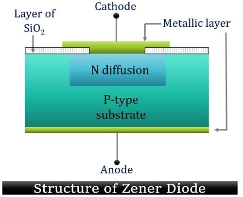
It is built using a heavily doped PN junction so that the depletion layer becomes very thin.
Thin depletion layer creates a strong electric field even at low reverse voltages.
The cathode is marked with a band, and the symbol has a bent line on the cathode side.
Because it is heavily doped, it can safely operate in breakdown without getting damaged.
Working Principle
Forward Bias
When the anode is connected to the positive terminal, it behaves like a normal diode.
Forward voltage drop in silicon Zener diode is about 0.7 V.
Reverse Bias
Initially, only a small leakage current flows.
As the reverse voltage increases and reaches the Zener voltage, the electric field becomes strong enough to pull electrons from covalent bonds.
At this point, the diode suddenly starts conducting a large current.
After breakdown, the voltage across the diode remains almost constant at the Zener voltage even if current changes.
Breakdown Mechanisms
Zener Breakdown
Occurs in heavily doped diodes.
Very thin depletion layer.
Strong electric field breaks covalent bonds and releases electrons.
Dominant below about 5–6 volts.
Avalanche Breakdown
Occurs in lightly doped diodes with a wide depletion layer.
Carriers gain high energy and create more carriers by collision.
Dominant above about 5–6 volts.
Zener diodes above 6 V commonly work by avalanche effect.
V-I Characteristics

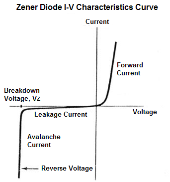
In forward region: behaves like a normal diode with ~0.7 V drop.
In reverse region: almost no current until Zener voltage.
At Zener voltage: sudden rise in reverse current (breakdown).
Voltage stays nearly constant at Vz during breakdown.
Formula Used in Voltage Regulation
Series Resistor (Rs) Calculation
Used to protect the Zener diode.
Rs=Vin−VzIz+ILR_s = \frac{V_{in} - V_z}{I_z + I_L}Rs=Iz+ILVin−Vz
where
VinV_{in}Vin = input voltage
VzV_zVz = Zener voltage
IzI_zIz = Zener current
ILI_LIL = load current
Applications
Used as a voltage regulator to supply a constant voltage to a load.
Used as a voltage reference in power supplies.
Used for over-voltage protection in circuits.
Used in clipping and clamping circuits for wave shaping.
Used in switching and timing circuits.
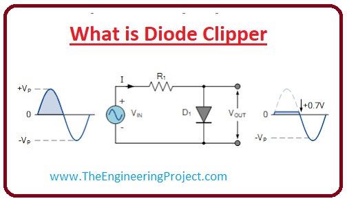
Clipping Circuits
A clipping circuit removes a selected portion of an AC input signal above or below a fixed reference level while keeping the rest of the waveform unchanged. It limits the amplitude of a signal without changing its frequency or basic shape.
Important points
The main purpose is to cut off or limit part of the waveform.
A diode is the core element that decides when current flows.
Some clippers work at zero level, others use a DC supply to clip at a chosen voltage.
Clipping can happen in either half cycle or both.
It is used in voltage protection, signal shaping, and digital conditioning.
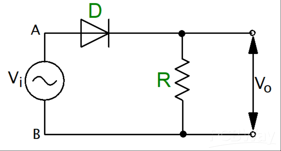
Construction of a Clipping Circuit
A diode is connected either in series or parallel with the load.
A resistor limits current and forms the output path.
In biased clippers, a DC voltage source is added in series with the diode.
Orientation of the diode decides whether the clipping is positive or negative.


Working Principle
When the input voltage makes the diode forward biased, the diode conducts and creates a short path, causing the output to be clipped.
When the input makes the diode reverse biased, the diode does not conduct, and the input appears at the output.
The reference level for clipping is determined by 0.7 V (silicon diode) or by the DC supply connected in the circuit for biased clippers.
Types of Clipping Circuits
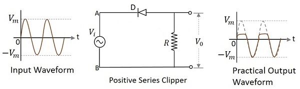
1. Series Clippers
The diode is placed in series with the load.
Clipping action occurs when the diode becomes forward-biased.
Provides less signal distortion compared to shunt clippers.
Types of series clippers:
Positive series clipper
Negative series clipper
Biased positive/negative series clipper
2. Shunt Clippers
The diode is placed parallel (shunt) to the load.
When the diode conducts, it diverts the current away from the load, clipping the voltage.
Simpler but may distort the waveform at high frequencies.
Types of shunt clippers:
Positive shunt clipper
Negative shunt clipper
Biased shunt clipper
Detailed Types
1. Positive Clipper

Removes the positive half cycle of the input.
Output contains only the negative part.
When the input becomes positive, diode conducts and clips the signal.
2. Negative Clipper
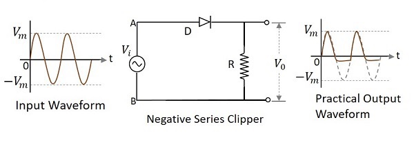
Removes the negative half cycle.
Output contains only the positive part.
Diode orientation is reversed compared to positive clipper.
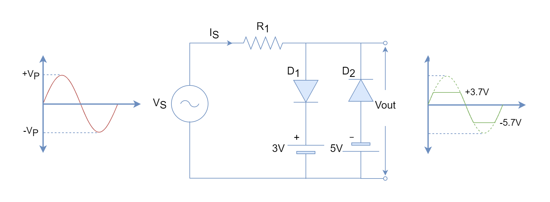
3. Biased Clippers


Uses a DC supply (Vb) to set the clipping level at any desired voltage.
Types of biased clippers:
Biased positive clipper
Biased negative clipper
4. Dual (Two-level) Clipper

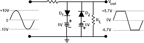

Clips both positive and negative peaks of the waveform.
One diode clips the top level, the other clips the bottom.
Used to keep the output within a fixed range.
Waveform Behavior (General Idea)
When diode conducts → output is cut (clipped).
When diode does not conduct → output follows input.
Biased diode shifts clipping point to a fixed voltage.
Dual clippers ensure the signal never crosses set upper and lower limits.
Applications
Protecting circuits from high voltage spikes.
Controlling voltage levels before ADC or digital circuits.
Shaping signals in communication systems.
Forming square and pulse waveforms.
Removing unwanted noise peaks.
Clamping Circuits
A clamping circuit shifts an entire AC waveform up or down so that either its maximum or minimum point touches a fixed DC level. It does not cut or remove any part of the waveform; instead, it adds a DC component to move the whole signal vertically without changing its shape.

6
Important points
A clamping circuit changes the DC level of a waveform.
The shape, frequency, and amplitude of the waveform remain the same.
It uses a diode, capacitor, and resistor as its main components.
The capacitor stores charge during one half cycle and releases it during the other, causing the waveform to shift.
The diode direction decides if the waveform is shifted upward or downward.
A DC supply can be added to shift the waveform to a desired level.
Construction
A diode is connected in series with the input signal.
A capacitor is connected parallel to the output path to store charge.
A resistor is connected to discharge the capacitor slowly and stabilize the output.
In biased clampers, a DC voltage source is added in series with the diode.
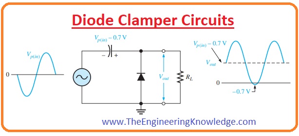
Working Principle
When the input signal makes the diode forward-biased, the diode conducts and the capacitor charges to a voltage close to the peak value of the input.
When the input changes direction and the diode becomes reverse-biased, the capacitor holds its previous charge.
Because of the capacitor voltage, the entire waveform is pushed up or down by an amount equal to the stored charge.
The capacitor value must be large enough so that its voltage does not discharge too quickly; otherwise, the clamping effect weakens.
The displacement of the waveform is approximately:
Types of Clamping Circuits
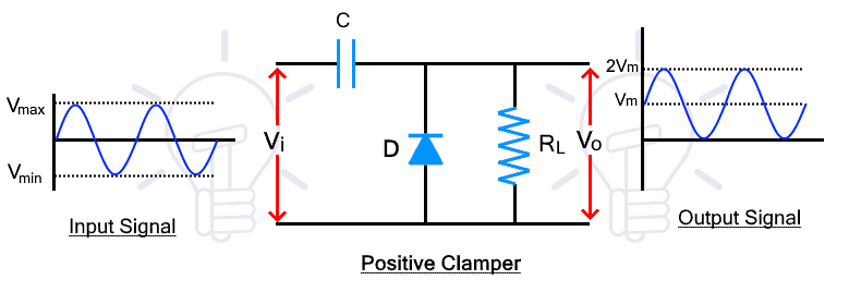
1. Positive Clamper
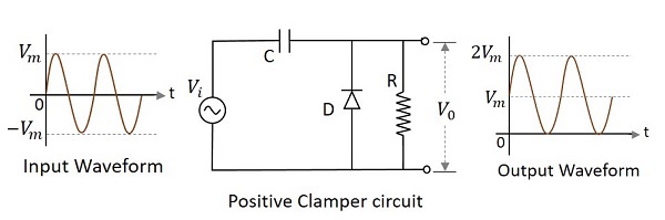
Shifts the entire waveform upward.
The negative peaks move to zero or above zero.
In this circuit, the diode conducts during negative half cycles and charges the capacitor.
The capacitor voltage then lifts the whole waveform upward.
2. Negative Clamper

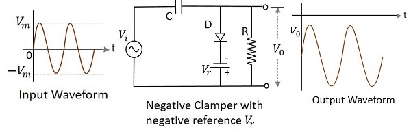
Shifts the entire waveform downward.
The positive peaks move to zero or below zero.
The diode conducts during positive half cycles and charges the capacitor.
The stored charge shifts the waveform downward.
3. Biased Clamper

Uses a DC voltage source to shift the waveform to a specific fixed level.
Used when a precise shift is required.
Waveform Behavior
The capacitor provides a stored voltage that adds to or subtracts from the input waveform.
The output waveform is displaced such that one of its peaks (positive or negative) touches the reference level.
The waveform shape remains the same; only its vertical position changes.
Applications
Restoring the DC level of signals in communication receivers.
Processing video signals to stabilize brightness levels.
Used in oscilloscopes to shift signals for display.
Peak detector and envelope detector circuits.
Waveform level shifting in amplifiers.